



Diamonds in Semiconductor Technology
As electronics design becomes more complex, enabling power efficiency in applications like electric vehicles (EVs) and artificial intelligence (AI) solutions becomes critical to maintaining robust and reliable products.
SiC and GaN have a bright future, but diamond could well proven to be the ultimate WBG (Wide band Gap) semiconductor material for applications in high-power electronics. Diamond is a perfect candidate for high-voltage operation, high-temperature applications or high-frequency switching. Diamond exhibits a critical electric field 30times higher than Si and 3times higher than SiC. It is also a very good heat dissipator, with a thermal conductivity 5times higher than copper.”
Considering the above benefits, recent days diamond wafers are emerging as a promising material for future semiconductor technology due to their unique properties, which could significantly impact the performance and efficiency of electronic devices. The properties of diamond are ideal for power devices and devices operating in extreme environments. Although diamond’s practical use has been limited by challenges in mass production, this situation continues to evolve, as numerous research institutions, including Gaayathri Innovative Technologies, have made significant advancements in diamond wafer production technology.
Diamond is an Ultimate thermal conductor & no other material conducts heat as efficiently as single-crystal diamond, enabling chips to run faster and last longer. In addition to this, diamond is also an Extreme electrical insulator. The thinnest slice of diamond insulates against very high voltages, enabling the next level of miniaturization in power electronics.
The chemical vapor deposition technique allows the synthesis of diamond in the shape of extended disks or wafers. Under optimized growth conditions the properties of these disks approach those of perfect diamond single crystals. In addition, the properties can be tailored according to the requirements of the manifold applications.
Diamond offers three key advantages over existing semiconducting materials:
- 1. Thermal management
- 2. Cost/efficiency optimization
- 3. CO2 reduction
When it comes to wafer downsizing, GIT is offering cutting-edge solutions for wafers, the best downsizing in terms of manufacturing smaller wafers or optimizing wafer yields for smaller chip production. We frequently work with 2” (50 mm), 3” (75 mm), 100 mm (4”), 125 mm (5”), 150 mm (6”), 200 mm (8”), and 300 mm wafers; however, we are also capable of producing custom non-standard sizes.
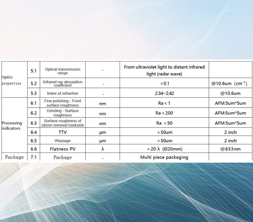
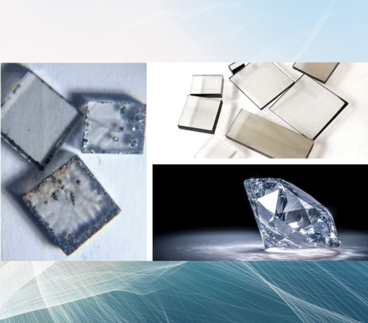
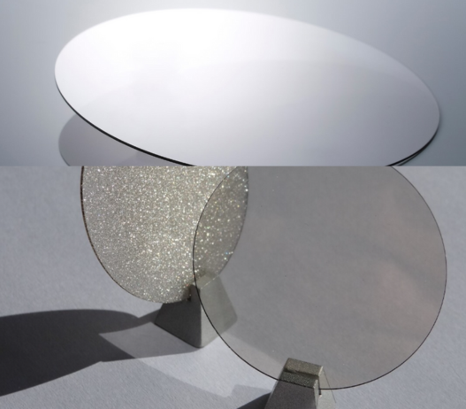
GIT Innovative
Diamond Wafers
The cooling system is a heavy and bulky part in all traditional power converters. Unlike most semiconductors, diamond has a decreasing resistivity with increasing temperature. Therefore, devices made from the material perform better at 150 degrees Celsius—the typical operating temperature for power devices than at room temperature. Whereas considerable effort must be expended to cool Si or SiC devices exposed to high operating temperatures, it is possible to simply let the diamond find a stable state during operation.
Diamond is also a good heat dissipator. With fewer losses to dissipate, better heat dissipation capability and the ability to operate at high temperature, converters made from active devices in diamond can be 5times lighter and smaller than Si-based solutions and 3times lighter and smaller than those based on SiC.
If the focus is on reducing device cost, it is possible to design a diamond die that is 30% less expensive than a SiC die, because a diamond die consumes up to 50time less diamond area than the equivalent SiC die for the same electrical performance and efficiency, but with better thermal management. If the focus is on efficiency, diamond can cut energy loss by a factor of three compared with SiC, with up to a 4times smaller die, allowing a direct savings in energy consumption.
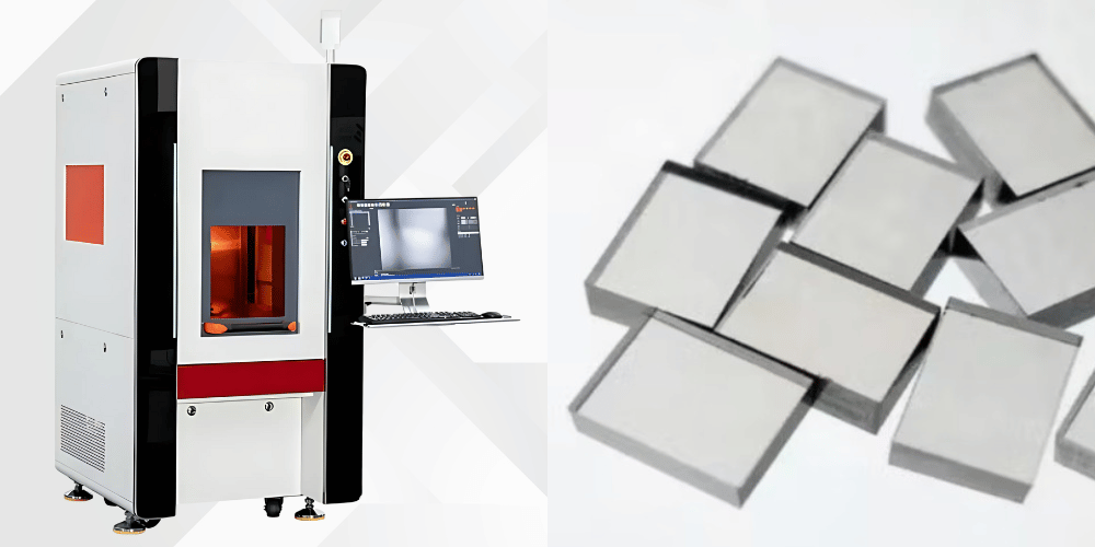
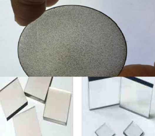
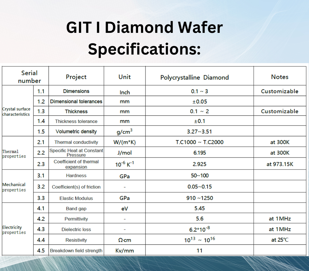
Diamond wafers from Gaayathri Innovative Technologies are wafer scale products that are used to tap the huge potential of diamond materials, such as tribological testing, nano-scale processing applications and MEMS development. In the current diamond wafer market, there are three grade diamond wafer