Laser SiC Dicing/Cutting

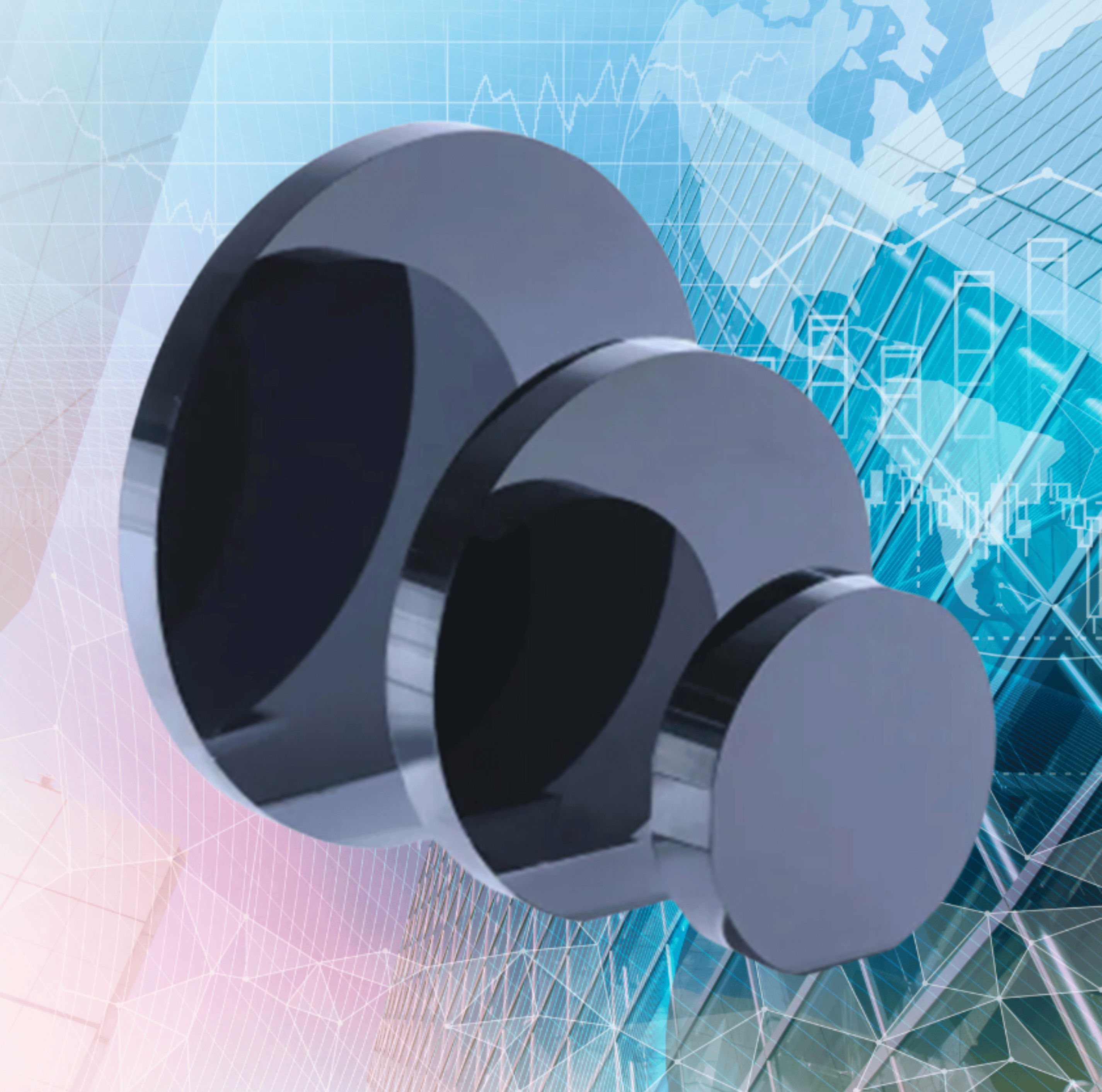
Today, the laser is an indispensable tool in modern production technology. Its precision, speed and non-contact process enable innovative processing options for almost all materials. This also applies to particularly demanding materials such as Silicon Carbide (SiC) - a high-tech ceramic that impresses with its hardness and resistance. This is precisely where GIT’s research into laser processes comes in.
GIT shed light on how different laser sources - from nanosecond, pico- and femtosecond to waterjet-guided laser technology - have been used to raise the quality standards in structuring, cutting and drilling SiC ceramics to a new level. Our work focuses on improving the surface and cutting quality as well as optimizing the removal rate.
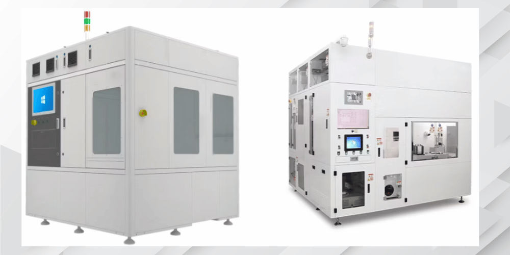
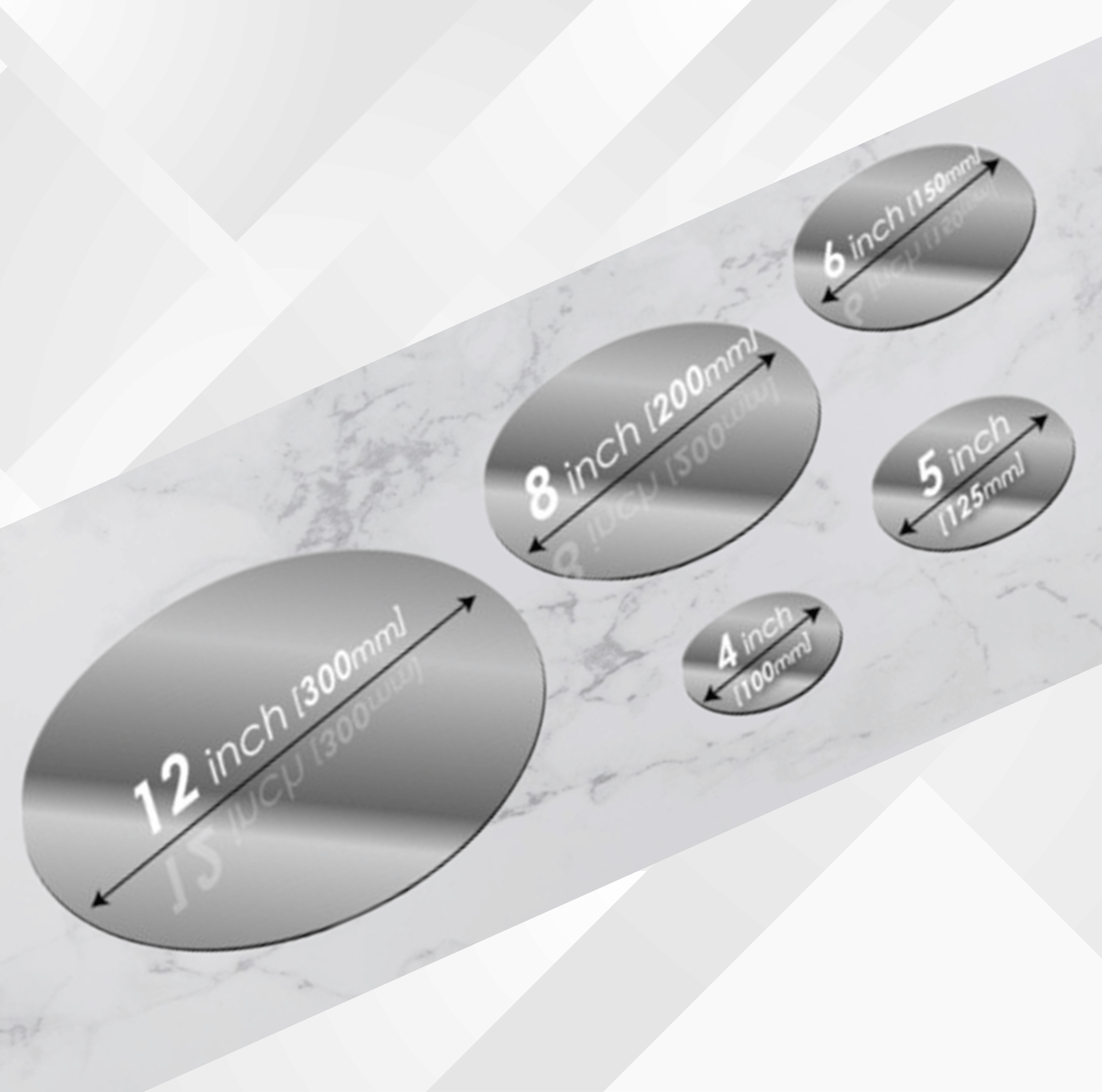
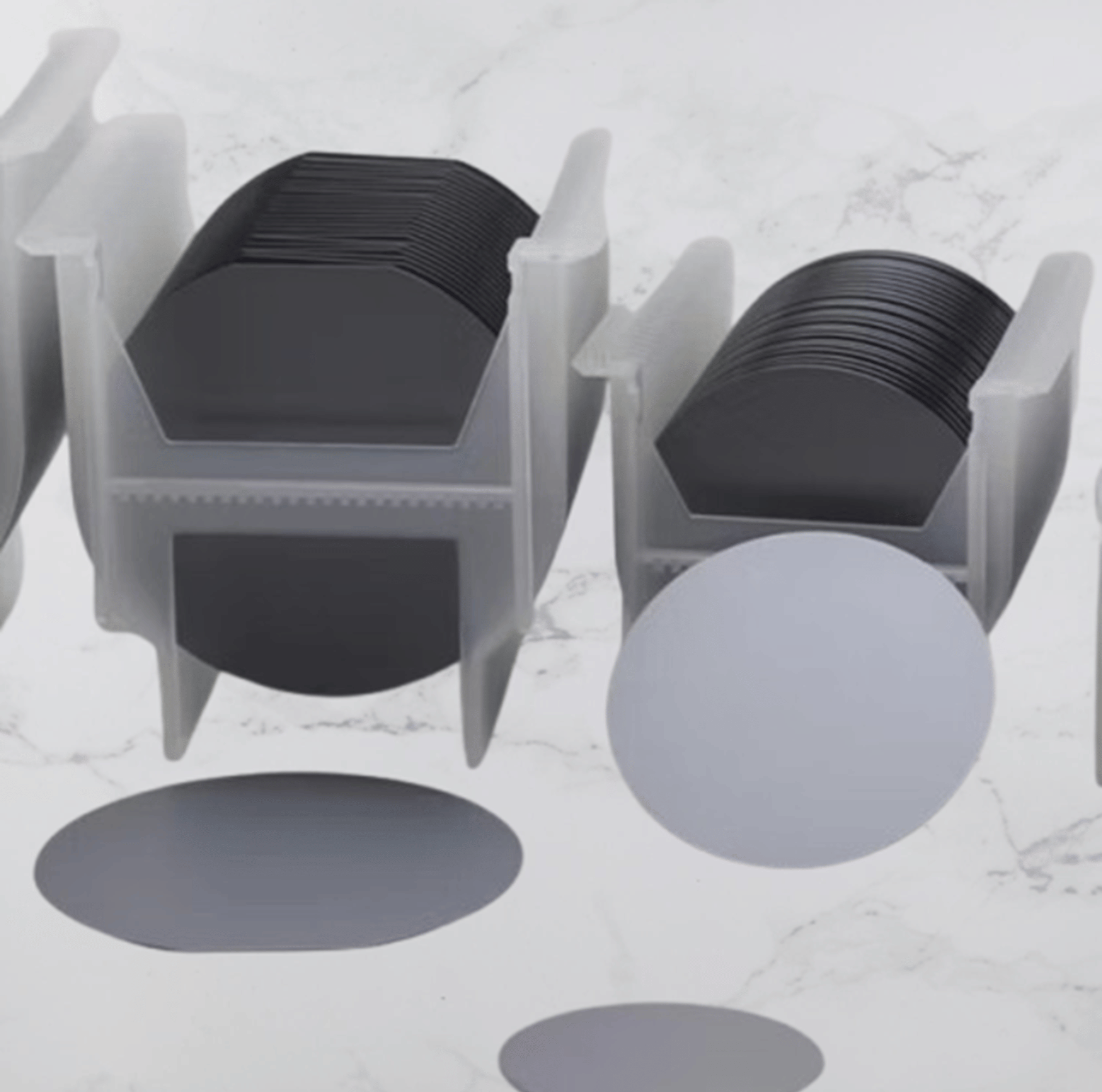
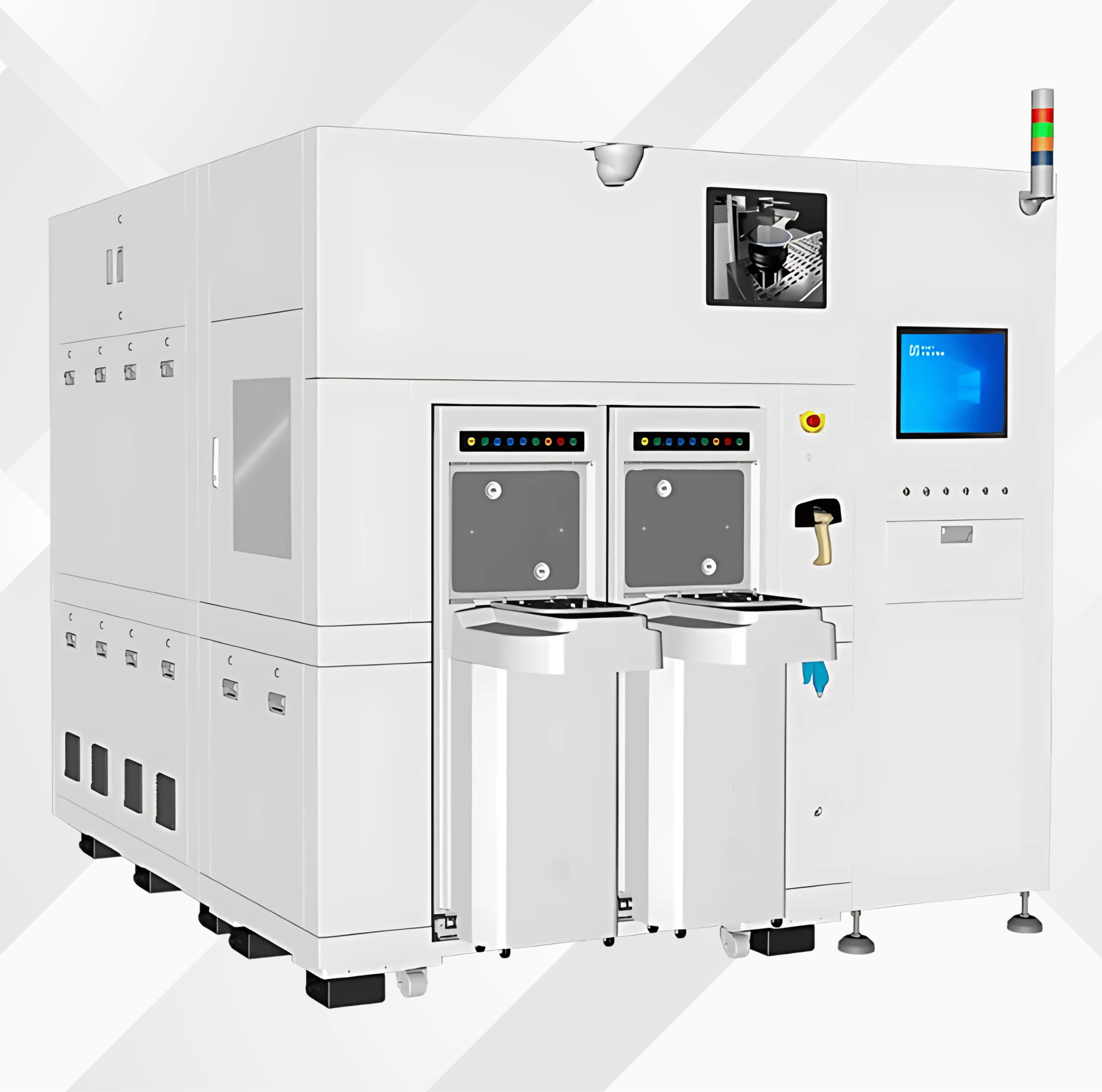
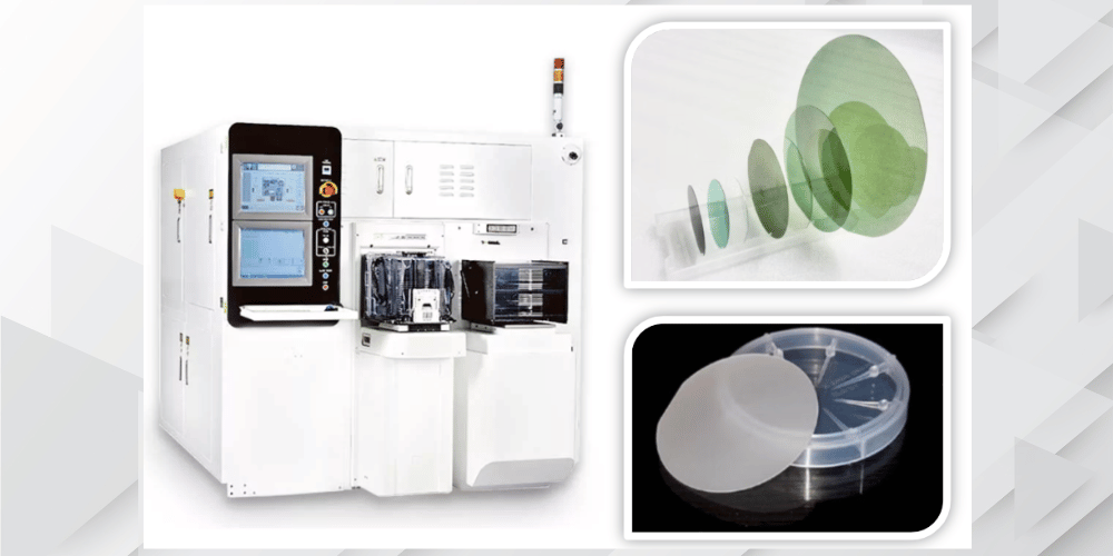
- The Fully Automatic SiC Wafer Modification and Cutting Equipment GIT Designed uses multiple high-precision CCD vision cameras to automatically identify and locate 6-8” inch wafers with various die specifications. Combining custom ultrafast lasers with a precision motion platform for relative movement, it performs internal wafer modification (stealth dicing). A dedicated wafer splitter then completes full wafer dicing and die separation.
- The system features a self-developed dynamic focus compensation module combined with a high-precision air-bearing linear motion platform, achieving industry-leading quality in high-precision, high-consistency wafer processing.
- Equipped with a standard-design black-box enclosed optical path for stealth dicing, it ensures stable laser beam transmission and energy output, providing excellent processing stability.
- With proprietary cutting and vision software, the system offers highly customizable functional modules to meet specific industry needs.
Product
Advantages
Cutting-Edge Technologies
Industries and Applications that Benefit with GIT Laser Technology